High-Performance Semiconductor Technology Leading the Green Transformation Integration of Sustainability Strategies and Technologies
As a world-class semiconductor silicon wafer supplier, Wafer Works Corporation is committed to providing global customers with high-quality products and services. Based on different component applications and end-use classifications, the Company combines the most suitable wafer materials and manufacturing technologies to deliver customized products and services. Leveraging core technologies accumulated over many years, the Company efficiently advances wafer size migration, shortens the technology development process, and rapidly enters target markets to establish a solid customer base.
Amid rapidly changing global trends and growing sustainability awareness, the Company continues to invest in advanced equipment and process optimization, making energy conservation, carbon reduction, and recycling no longer merely supplementary indicators, but rather natural outcomes derived from its core manufacturing capabilities.
Among its key products, heavily doped N-type silicon substrates are one of Wafer Works' principal offerings, and their quality has reached world-class standards, enabling stable supply to major N-type substrate customers worldwide. The continuous development of low-energy-consumption and higher-efficiency N-type substrates has always been one of the Company's ongoing goals. When the resistivity of N-type silicon substrates becomes lower, it indicates better conductivity, which offers significant
advantages for manufacturing certain types of power devices and high-speed electronic components. This not only helps users improve energy efficiency, but also contributes to environmental sustainability.
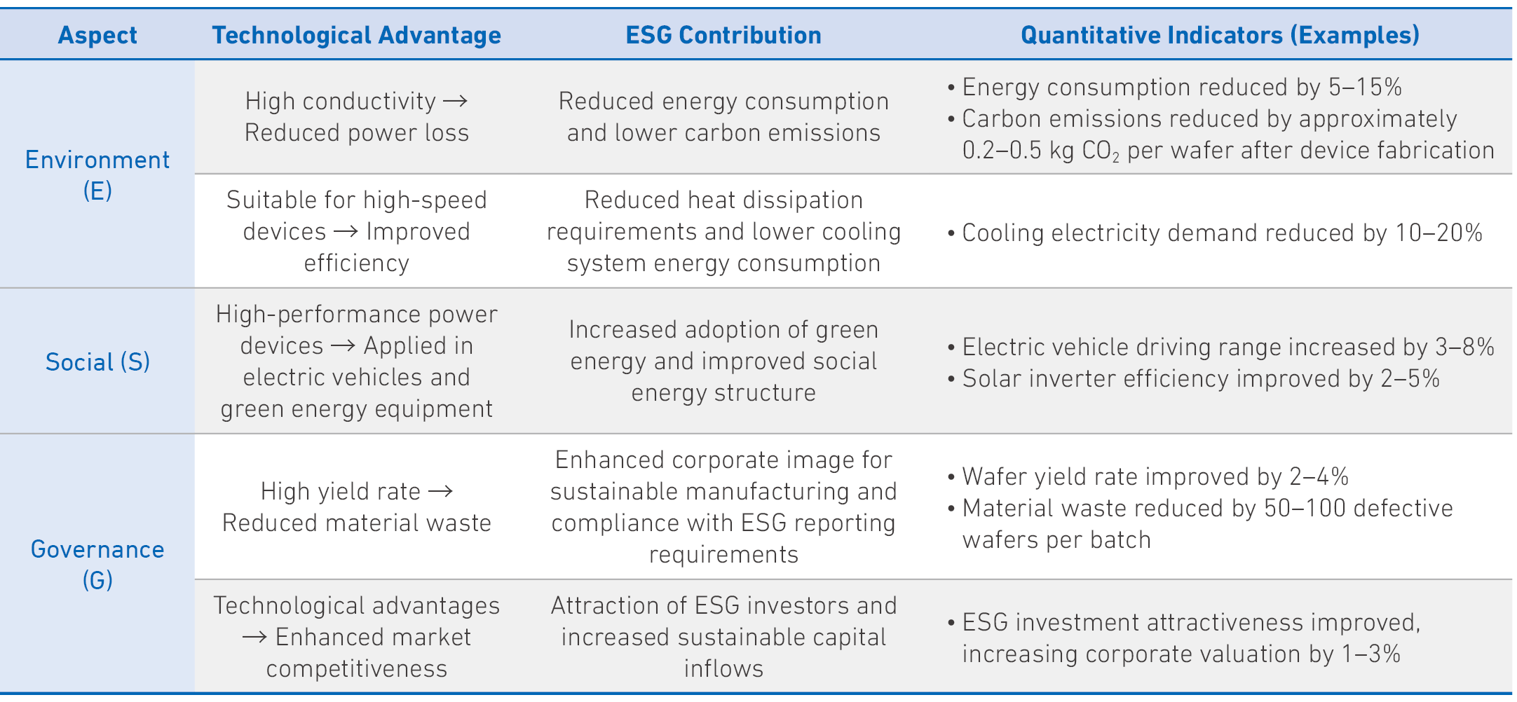
ESG Performance: Technological Advantages and Quantifiable Contributions
Wafer Works transforms its leading process technologies into measurable ESG impacts, as illustrated below:
Key Breakthrough: Environmental Leadership Through Ultra-High Doping Technology
Wafer Works has successfully advanced N-type semiconductor substrates from the ultra-low resistivity range (0.001–0.01 Ω·cm) into the ultra-high doping range (< 0.001 Ω·cm), enabling each wafer to further reduce carbon emissions by approximately 30 kg of CO2. This achievement significantly enhances carbon reduction efficiency per unit.
Carbon Reduction Achievements:
Based on an annual production scale of 100,000 ultra-high-doping wafers, the environmental contributions are as follows:
- Total annual carbon reduction: an additional reduction of 3,000 metric tons (3,000,000 kg) of CO2 emissions.
- Natural offset value:
。 Equivalent to the annual carbon sequestration effect of planting 250,000 mature trees.
。 Equivalent to the total natural carbon absorption capacity of approximately 8 Daan Forest Park (approximately 130 hectares of green space).
Future Outlook: Five Major Advantages of Low-Resistivity N-Type Silicon Substrates
As a world-class semiconductor silicon wafer supplier, Wafer Works continues to develop materials with even lower resistivity to help users improve energy efficiency:
1. Ultimate Energy Conversion Efficiency: Significantly reduces conduction loss and achieves outstanding conversion efficiency.
2. Superior Thermal Management: Reduces device heat generation and lowers the energy demand of cooling systems.
3. Support for High-Frequency Applications: Optimizes carrier concentration to meet the requirements of 5G and high-speed computing.
4. Extended System Lifespan: Reduces thermal stress and enhances the durability and reliability of end products.
5. Empowering Green Supply Chains: Directly supports performance improvements in electric vehicles and green energy equipment.