Product Layout
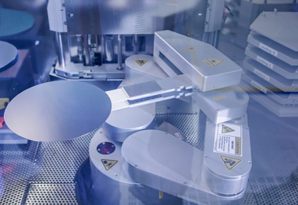
As a globally renowned supplier of semiconductor silicon wafers, Wafer Works has been dedicated to providing top-notch products and services to customers. Our products include 12-inch (and below) polished wafers, epitaxial wafers, double-side wafers, lapped wafers, etched wafers, ultra-thick and ultra-thin wafers, and SOI wafers, with various doping choices. Moreover, we offer customers the most suitable products and services tailored to the unique requirements of different applications. Drawing on our expertise in materials and our integrated technology spanning crystal growth to epitaxial deposition, we ensure that we meet and exceed our customers' present and future needs. Take 8-inch products as an example, the below graph illustrates the product layout we offer, which is categorized based on a wide range of components and end applications. Each category is thoughtfully matched with the most suitable materials and production technology, enabling us to deliver highly customized products and services. We provide a similar product layout for wafers in other sizes as well. For more information and details, please feel free to contact us.

|
Specific Polished wafer type From ultra-low to ultra-high resistivity
Example of device MEMS, power MOSFET, PMIC(power management IC) and more
|
Power Polished wafer type low resistivity or ultra-low resistivity
Example of device power MOSFET, BJT, diode, thyristor, IGBT, CoolMOS, superjunction and more
|
Imaging Polished wafer type low resistivity
Example of device Image sensor, CIS(COMS image sensor) and more
|
|
Analog Polished wafer type Lightly doped wafer
Example of device LED driver, PMIC(power management IC) and more
|
Logic Polished wafer type Lightly doped wafer
Example of device Standard logic IC and ASIC(application specific IC)
|
RF Polished wafer type Ultra-high resistivity
Example of device RF devices
|

Technology Platform
With a comprehensive product layout, Wafer Works has amassed self-developed skills and expertise, encompassing various stages from crystal growth to epitaxial deposition. The table below outlines the essential technologies we possess.
|
|
Wafer Technology
|
Epitaxial Technology
|
Technology Development
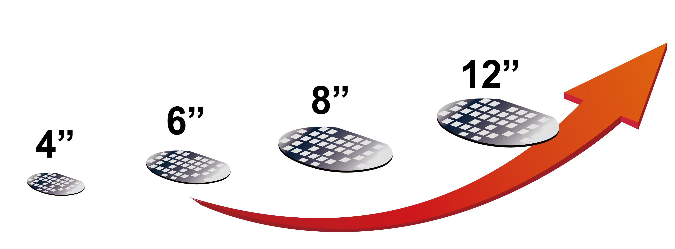
Wafer Works sets its sights on becoming a leading supplier of semiconductor silicon wafers, being determined to achieve self-development in cutting-edge technologies. Apart from establishing a comprehensive product layout, we are committed to driving the efficient progression of wafer dimension development, which shortens the timelines for technological research, innovation, and development, enabling us to swiftly enter target markets and cultivate a strong customer base.