产品布局
合晶科技作为世界级半导体用硅片供货商,致力于提供全球顾客高质量的产品与服务,产品包括各种掺质12寸(含以下)的抛光硅片、外延硅片、双抛硅片、研磨硅片、蚀刻硅片、超薄硅片及SOI硅片,并针对不同应用的组件特性,以自身的材料专业及由长晶至磊晶的整合技术,为客户提供最适当的产品与服务,满足客户现在与未来的需求。 以8寸产品为例,下图为合晶科技半导体硅片的产品布局,依据不同组件用途与终端应用的分类,搭配最适当的硅片材料及生产技术,提供定制化的产品与服务。其余尺寸硅片亦有相似的产品布局,请连络我们获得进一步的信息。

|
Specific Polished wafer type From ultra-low to ultra-high resistivity
Example of device MEMS, power MOSFET, PMIC(power management IC) and more
|
Power Polished wafer type low resistivity or ultra-low resistivity
Example of device power MOSFET, BJT, diode, thyristor, IGBT, CoolMOS, superjunction and more
|
Imaging Polished wafer type low resistivity
Example of device Image sensor, CIS(COMS image sensor) and more
|
|
Analog Polished wafer type Lightly doped wafer
Example of device LED driver, PMIC(power management IC) and more
|
Logic Polished wafer type Lightly doped wafer
Example of device Standard logic IC and ASIC(application specific IC)
|
RF Polished wafer type Ultra-high resistivity
Example of device RF devices
|

技术平台
为使产品布局完整,合晶科技已积累完备的自主技术,领域涵盖晶棒成长至外延,当中关键技术如下表所列。
|
|
抛光硅片技术
|
外延硅片技术
|
技术发展
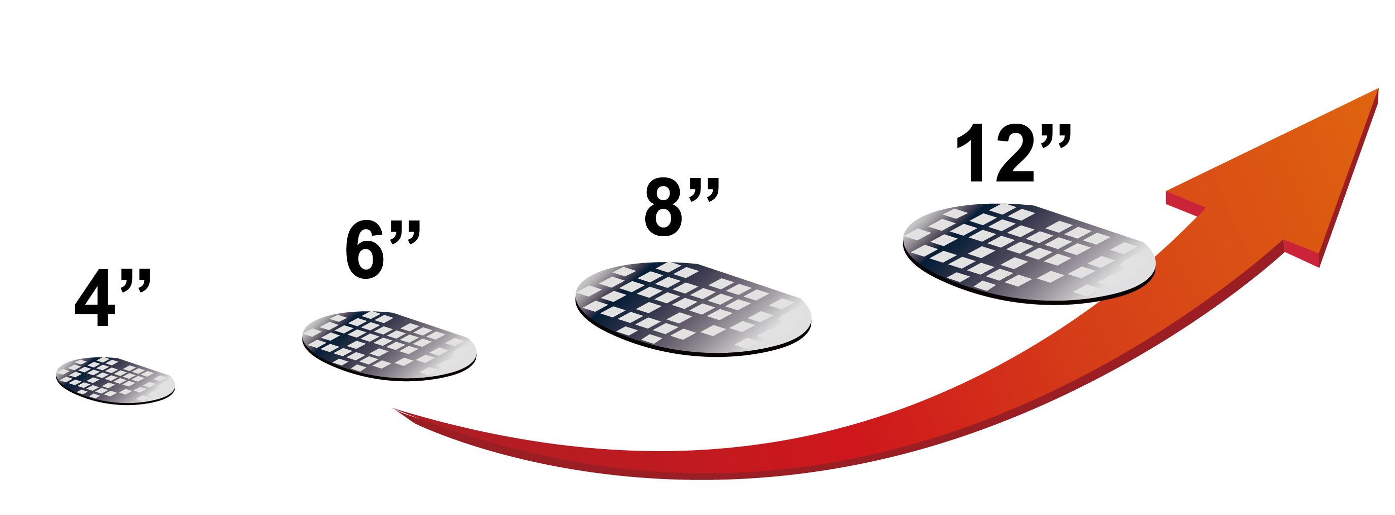
合晶科技期望成为国际级半导体硅片领头供货商,除了在市场占有一定的份额外,更要达到技术自主与领先。除了有效将产品完整的布局并拓展市场份额之外,更是以长年积累的核心技术有效率地推进尺寸的跃升,缩短技术研发的过程,快速地进入目标市场奠定客户基础。